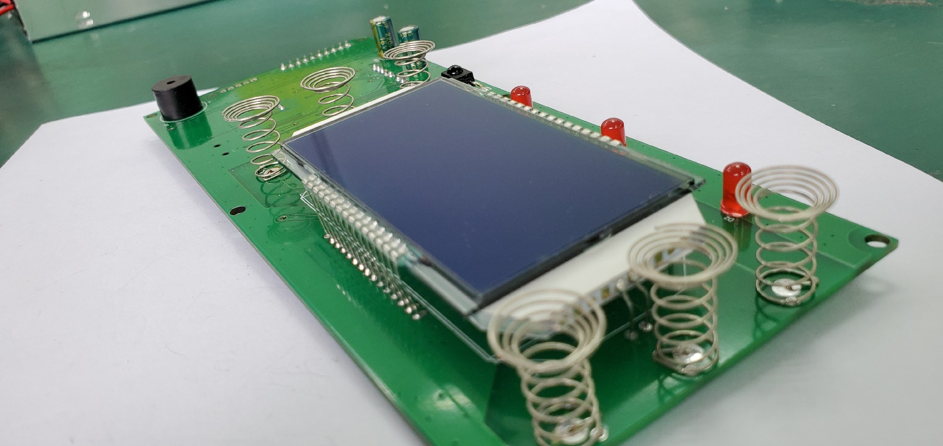
What are the PCBA processing and packaging technologies
PCBA processing and packaging technology is an important part of modern electronic manufacturing, which involves the installation and packaging of electronic components on the printed circuit board (PCB) to form a complete circuit system. There are a variety of packaging technologies commonly used in PCBA processing, and each technology has its unique characteristics and application scenarios. Here are some of the main packaging technologies:
1.DIP (Dual In-line Package) : Dual in-line package, which is one of the earliest chip packaging forms. Pins lead from both sides of the package in a linear arrangement. DIP package has the advantages of simple structure, easy to plug and unplug, but the number of pins is limited, and it is not suitable for high-density packaging.
2.QFP (Quad Flat Package) : four-sided flat package, is a surface mount type package form. The pins lead from four sides in a flat shape. QFP package has many pins, small size, light weight and other advantages, suitable for high-density assembly.
3.PLCC (Plastic Leaded Chip Carrier) : plastic leaded chip carrier, which is also a surface mount type package form. The pins lead from the four sides of the package in a J shape. PLCC package has many pins, high reliability, easy to automate production and so on.

4.BGA (Ball Grid Array) : Ball grid array package, is a high-density surface mount type package form. Pins are arranged in a spherical array at the bottom of the package. BGA package has the advantages of large number of pins, small space, good heat dissipation, etc., which is suitable for high performance and high density electronic products.
5.CSP (Chip Scale Package) : chip level package, is a very small surface mount type package form. The package size is similar to the chip size, and the pin spacing is very small. CSP package has the advantages of small size, light weight and low power consumption, which is suitable for portable electronic products.
6.SOIC (Small Outline Integrated Circuit) : small outline integrated circuit package, the pins lead from both sides of the package, in a curved shape. SOIC package has the advantages of moderate pin number, small size, light weight, etc., and is suitable for general density electronic products.
7.SOP (Small Outline Package) : a small outline package with pins drawn from one side of the package and arranged in a linear manner. SOP packages are similar to SOIC packages, but with larger pin spacing and are suitable for components with fewer pins.
8.TSSOP (Thin Shrink Small Outline Package) : thin small outline package, the pins lead from both sides of the package, in a linear arrangement, but the pin spacing is smaller than SOP. TSSOP package has the advantages of small size, light weight and suitable for high-density assembly.
9.QFN (Quad Flat No-lead Package) : four-sided pin-less flat package, is a pin-less surface mount package form. Pins are soldered directly to the board, no additional pin inserts are required. QFN package has the advantages of small size, light weight, good heat dissipation, etc., suitable for high performance, high density electronic products.


