

SOLUTION
Product Display
PCB sampling
Author:wangfan Source:本站 Release time:2024-03-05 Browse:504
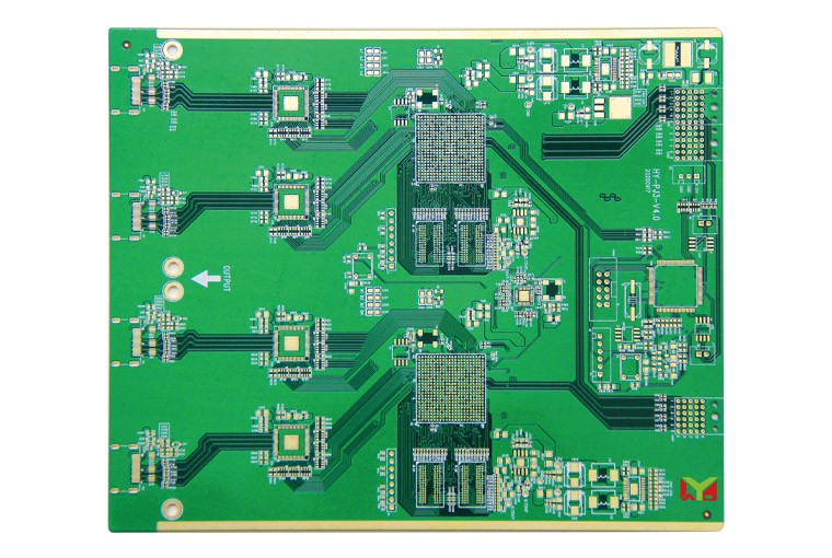
PCB means printed circuit board, also known as printed circuit board or printed circuit board, which is an important electronic component. As a support for electronic components, it provides electrical connections for electronic components. Because it is made using electronic printing, it is called a "printed" circuit board. PCB prototyping refers to the trial production of printed circuit boards before mass production. It generally refers to electronic products that are sent to pcb manufacturers for processing into pcb boards after engineers complete the pcb layout design. The update and iteration of electronic products is relatively fast, so the demand for pcb prototyping is also gradually growing, and the market share is constantly expanding. As the process requirements of electronic products are getting higher and higher, information is getting faster and faster, resulting in multi-layer PCB prototyping. The rise is relatively fast.
1 PCB proofing process
PCB prototyping tools/raw materials
Plate materials available: PR4, CEM-1, 94V-0, aluminum substrate, etc.
Copper thickness optional: 0.5OZ, 1OZ, 2OZ, etc.
The specific process of PCB proofing is as follows:
1. Contact the PCB proofing manufacturer
First, you need to inform the manufacturer of the documents, process requirements, and quantity.
Taking Huaqiang PCB Factory as an example, first enter the official website, then register a customer number, and then you can choose to quote online, place an order, and follow up on the production progress. Manual service is also available.
2. Open materials
Purpose: According to the requirements of the engineering data MI, cut the large sheets that meet the requirements into small pieces to produce panels. Small pieces of sheet metal that meet customer requirements.
Process: large sheet → cutting according to MI requirements → curium board → filleting\edge grinding → plate output
3. Drilling
Purpose: According to the engineering data, drill the required hole diameter at the corresponding position on the sheet metal that meets the required size.
Process: Stacking pins → Upper plate → Drilling → Lower plate → Inspection\repair
4. Immersed copper
Purpose: Copper deposition is to use chemical methods to deposit a thin layer of copper on the wall of the insulating hole.
Process: Rough grinding → Hanging plate → Copper immersing automatic line → Lower plate → Dip 1% dilute H2SO4 → Thickening copper
5. Graphic transfer
Purpose: Graphic transfer is to transfer the image on the production film to the board
process:
(Blue oil process): Grind the plate → Print the first side → Dry → Print the second side → Dry → Expose → Develop → Inspect;
(Dry film process): Linen board → Lamination → Rest → Alignment → Exposure → Rest → Develop → Inspection
6. Graphic plating
Purpose: Graphic plating is to electroplat a layer of copper with a required thickness and a gold, nickel or tin layer with a required thickness on the exposed copper of the circuit pattern or on the hole wall.
Process: Placing the board → Degreasing → Washing twice → Micro-etching → Washing → Pickling → Copper plating → Washing → Pickling → Tin plating → Washing → Lowering the board
7. Remove film
Purpose: Use NaOH solution to remove the anti-electroplating covering layer to expose the non-circuit copper layer
Process: water film: insert rack → soak in alkali → rinse → scrub → pass through the machine; dry film: place the plate → pass through the machine
8. Etching
Purpose: Etching is to use chemical reaction to corrode the copper layer in non-circuit parts.
9. Green oil
Purpose: Green oil is to transfer the graphics of the green oil film to the board, which plays a role in protecting the circuit and preventing tin on the circuit when welding parts.
Process: Grind the plate → Print photosensitive green oil → Curium plate → Expose → Develop; Grind the plate → Print the first side → Bake the plate → Print the second side → Bake the plate
10. Characters
Purpose: The character is a mark provided for easy identification
Process: After curing the green oil → Cooling and letting stand → Adjusting the screen → Printing characters → Curing
11. Gold-plated fingers
first step:
Purpose: To plate a nickel/gold layer of required thickness on the plug fingers to make them more hard and wear-resistant
Process: plate loading → oil removal → water washing twice → micro-etching → water washing twice → pickling → copper plating → water washing → nickel plating → water washing → gold plating.
Step two:
Tin plate (a parallel process)
Purpose: Tin spraying is to spray a layer of lead and tin on the exposed copper surface that is not covered with solder mask oil to protect the copper surface from corrosion and oxidation and ensure good soldering performance.
Process: micro-etching → air drying → preheating → rosin coating → solder coating → hot air smoothing → air cooling → washing and air drying
12. Forming
Purpose: To mold the shape into the shape required by the customer through mold stamping or CNC machine, using organic gongs, beer boards, hand gongs, and hand cutting.
Explanation: The precision of data cutter board and beer board is higher, hand cutter board is second, and hand cutter board can only make some simple shapes at the lowest.
13. Test
Purpose: Through 100% electronic testing, detect open circuits, short circuits and other defects that affect functionality that are not easily found visually.
Process: Upper mold→Place the board→Test→Qualified→FQC visual inspection→Unqualified→Repair→Return to test→OK→REJ→Scrap
14. Final inspection
Purpose: To avoid the leakage of problematic and defective panels through 100% visual inspection of panel appearance defects and repair of minor defects.
Specific work flow: Incoming materials → View information → Visual inspection → Qualified → FQA spot check → Qualified → Packaging → Unqualified → Processing → Check OK
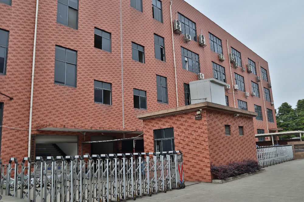
- ABOUT US Company Profile Workshop Display R&D Strength Stuff Member
- PRODUCT Electronic Ballast PCBA Processing Membrane Switch Solution
- SOLUTION Product Catalog News R&D Sharing Water Treatment Solutions Technical Answer Trade Cooperation
- CONTACT US Contact Information Message Cooperation Intention

Jenny Wong
SOCIAL


Copyright © 2024 Sichuan Baichuan Technology Co., Ltd ICP12345678 XML地图